


December 16, 2025 · 24-Hour AI Briefing: High NA EUV Goes Live, B300 Enters Real Deployment, and the NVIDIA–TPU Platform Battle Intensifies
Over the past 24 hours, three developments across AI and semiconductors stood out as clear inflection points rather than routine updates. Intel and ASML completed acceptance testing for the world’s first second-generation High NA EUV system. NVIDIA’s Blackwell Ultra–based B300 GPUs entered a live production network serving real users. And NVIDIA publicly reinforced its narrative of platform leadership over Google’s TPU.
Together, these signals point to a deeper shift: AI competition is no longer about raw compute scale alone, but about manufacturing leverage, system delivery, and platform choice.
1. Intel completes acceptance of second-generation High NA EUV, reshaping advanced-node dynamics
Intel announced that it has completed unboxing and acceptance testing of the industry’s first second-generation High Numerical Aperture (High NA) EUV lithography system in collaboration with ASML. The new tool features a higher-power EUV light source, wafer throughput of up to 175 wafers per hour, overlay accuracy improved to 0.7nm, and enhanced wafer handling for greater stability.
Commentary:
This is far more than a routine equipment milestone. High NA EUV represents a potential rebalancing point in the global advanced-manufacturing power structure. Its core value lies in using a higher numerical aperture to compress the most expensive, slowest, and most fragile layers of multi-patterning within the same process node—reducing both process complexity and yield risk.
For Intel, this creates an opportunity to reshape both the cost curve and the cycle time curve beyond the 18A and 14A roadmap. If fewer patterning steps can deliver equal or better linewidth control and overlay precision, ramp speed improves and per-wafer cost becomes more predictable—an especially critical factor for Intel Foundry Services (IFS) as it seeks external customers.
Whether High NA translates into sustained, scalable leadership will ultimately depend on execution across materials, process integration, and variability control. The question remains open: can Intel use this window to meaningfully challenge TSMC’s dominance?
2. AlphaTON Capital deploys NVIDIA B300 into Telegram’s AI network
AlphaTON Capital announced that it has received its first batch of NVIDIA B300 GPUs, integrating them into Supermicro’s HGX liquid-cooled systems to enhance the Cocoon AI network, which will deliver privacy-focused AI services to Telegram users.
Commentary:
The B300 is currently among the most powerful AI accelerators available. Built on the Blackwell Ultra architecture, it delivers up to 144 PFLOPS of FP4 compute and features 288GB of HBM3e memory, optimized for long-context inference. Supermicro’s liquid-cooling platform enables up to 98% heat recovery and roughly 40% energy-efficiency gains, making ultra-dense deployment feasible.
For AlphaTON, this move secures leading-edge compute while also mitigating geopolitical and supply-chain risk. Telegram’s Cocoon network previously relied heavily on community nodes, raising questions around scale and stability. Integrating B300 shifts the strategy toward tightly coupling high-end AI infrastructure with the Telegram ecosystem, aiming to build an “AI + blockchain + privacy” closed loop.
That said, open questions remain. Long-term B300 supply sustainability and regulatory compliance around privacy-preserving AI across jurisdictions will become decisive factors as the network scales.
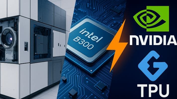
3. NVIDIA reinforces its lead over TPU as the platform battle heats up
Following meetings with NVIDIA’s investor relations team, Bernstein reported that NVIDIA believes its technology stack leads Google’s TPU by roughly two years, emphasizing the flexibility of GPUs in building large-scale cloud AI infrastructure.
Commentary:
A simple “two-year lead” framing oversimplifies the reality. TPUs are deeply co-designed around Google’s most critical internal models and operators, allowing them to match or even exceed GPUs in specific workloads. GPUs, by contrast, derive their advantage from breadth: ecosystem maturity, tooling, and rapid adaptability to new model architectures.
With TPU v7 delivering major efficiency gains and demonstrating impressive linear scaling across tens of thousands of accelerators, NVIDIA’s messaging is clearly aimed at reinforcing the narrative of general-purpose GPUs as irreplaceable infrastructure.
Yet the landscape is shifting. Gemini 3 is trained entirely on TPU, and Meta has begun testing TPU-hosted models. If more hyperscalers migrate toward in-house or semi-custom silicon, NVIDIA’s role as the “default” AI infrastructure provider will inevitably narrow.
As AI transitions from research experimentation to industrial deployment, winners will be determined less by peak theoretical performance and more by who enables customers to run production workloads faster, more reliably, and at lower cost. CUDA’s ecosystem lock-in remains NVIDIA’s strongest moat—but for customers, more platforms and more choice are clearly beneficial.
Past 72 Hours: AI Developments Worth Revisiting
For broader context, readers may also explore:
Conclusion
From High NA EUV entering real manufacturing, to B300 powering live user networks, to the intensifying GPU–TPU platform debate, one message is clear: AI competition has moved beyond “who has more compute” to “who controls manufacturing, systems, and choice.”
The next generation of leaders will not simply design the fastest chips. They will be the players capable of integrating process technology, compute, energy, system delivery, and ecosystem leverage into repeatable, scalable capacity.
The second half of the AI race has officially begun.